- 您现在的位置:买卖IC网 > Sheet目录312 > AT25F4096W-10SU-2.7 (Atmel)IC FLASH 4MBIT 33MHZ 8SOIC
�� �
�
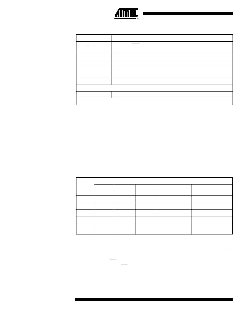
�Table� 7.� Read� Status� Register� Bit� Definition�
�Bit�
�Bit� 0� (RDY)�
�Bit� 1� (WEN)�
�Bit� 2� (BP0)�
�Bit� 3� (BP1)�
�Bit� 4� (BP2)�
�Definition�
�Bit� 0� =� “0”� (RDY)� indicates� the� device� is� READY.� Bit� 0� =� “1”� indicates� the�
�write� cycle� is� in� progress.�
�Bit� 1� =� “0”� indicates� the� device� is� not� WRITE� ENABLED.� Bit� 1� =� “1”�
�indicates� the� device� is� WRITE� ENABLED.�
�See� Table� 8.�
�See� Table� 8.�
�See� Table� 8.�
�Bits� 5-6� are� 0s� when� device� is� not� in� an� internal� write� cycle.�
�Bit� 7� (WPEN)�
�See� Table� 9.�
�Bits� 0-7� are� 1s� during� an� internal� write� cycle.�
�READ� PRODUCT� ID� (RDID):� The� RDID� instruction� allows� the� user� to� read� the� manufac-�
�turer� and� product� ID� of� the� device.� The� first� byte� after� the� instruction� will� be� the�
�manufacturer� code� (1FH� =� ATMEL),� followed� by� the� device� code� 64H.�
�WRITE� STATUS� REGISTER� (WRSR):� The� WRSR� instruction� allows� the� user� to� select�
�one� of� five� levels� of� protection� for� the� AT25F4096.� The� AT25F4096� is� divided� into� eight�
�sectors� where� the� top� 1/8,� top� quarter� (1/4),� top� half� (1/2),� or� all� of� the� memory� sectors�
�can� be� protected� (locked� out)� from� write.� Any� of� the� locked-out� sectors� will� therefore� be�
�read� only.� The� locked-out� sector� and� the� corresponding� status� register� control� bits� are�
�shown� in� Table� 8� on� page� 8.�
�The� four� bits,� BP0,� BP1,� BP2� and� WPEN,� are� nonvolatile� cells� that� have� the� same� prop-�
�erties� and� functions� as� the� regular� memory� cells� (e.g.,� WREN,� t� WC� ,� RDSR).�
�Table� 8.� Block� Write� Protect� Bits�
�Status� Register� Bits�
�AT25F4096�
�Array� Addresses�
�Level�
�0(none)�
�1(1/8)�
�2(1/4)�
�3(1/2)�
�4(all)�
�BP2�
�0�
�0�
�0�
�0�
�1�
�BP1�
�0�
�0�
�1�
�1�
�x�
�BP0�
�0�
�1�
�0�
�1�
�x�
�Locked� Out�
�None�
�070000� -� 07FFFF�
�060000� -� 07FFFF�
�040000� -� 07FFFF�
�000000� -� 07FFFF�
�Locked-out� Sector(s)�
�None�
�Sector� 8�
�Sector� 7,� 8�
�Sector� 5,� 6,� 7,� 8�
�All� sectors�
�(1� -� 8)�
�Note:�
�1.� x� =� don’t� care�
�The� WRSR� instruction� also� allows� the� user� to� enable� or� disable� the� write� protect� (WP)�
�pin� through� the� use� of� the� write� protect� enable� (WPEN)� bit.� Hardware� write� protection� is�
�enabled� when� the� WP� pin� is� low� and� the� WPEN� bit� is� “1”.� Hardware� write� protection� is�
�disabled� when� either� the� WP� pin� is� high� or� the� WPEN� bit� is� “0.”� When� the� device� is� hard-�
�ware� write� protected,� writes� to� the� status� register,� including� the� block� protect� bits� and� the�
�WPEN� bit,� and� the� locked-out� sectors� in� the� memory� array� are� disabled.� Write� is� only�
�allowed� to� sectors� of� the� memory� which� are� not� locked� out.� The� WRSR� instruction� is�
�self-timed� to� automatically� erase� and� program� BP0,� BP1,� BP2� and� WPEN� bits.� In� order�
�8�
�AT25F4096�
�2454G–SFLSH–5/06�
�发布紧急采购,3分钟左右您将得到回复。
相关PDF资料
AT25HP512W2-10SI-2.7 SL383
IC EEPROM 512KBIT 10MHZ 16SOIC
AT26DF081A-SSU
IC FLASH 8MBIT 70MHZ 8SOIC
AT26DF161-SU
IC FLASH 16MBIT 66MHZ 8SOIC
AT26DF161A-MU
IC FLASH 16MBIT 70MHZ 8QFN
AT26DF321-SU
IC FLASH 32MBIT 66MHZ 8SOIC
AT27BV010-90JU
IC OTP 1MBIT 90NS 32PLCC
AT27BV020-90JU
IC OTP 2MBIT 90NS 32PLCC
AT27BV040-12JU
IC OTP 4MBIT 120NS 32PLCC
相关代理商/技术参数
AT25F4096Y4-10YH-2.7
制造商:ATMEL 制造商全称:ATMEL Corporation 功能描述:4Mbit High Speed SPI Serial Flash Memory
AT25F512
制造商:ATMEL 制造商全称:ATMEL Corporation 功能描述:SPI Serial Memory
AT25F512_04
制造商:ATMEL 制造商全称:ATMEL Corporation 功能描述:SPI Serial Memory
AT25F512A
制造商:ATMEL 制造商全称:ATMEL Corporation 功能描述:SPI EEPROM Product Qualification
AT25F512A_06
制造商:ATMEL 制造商全称:ATMEL Corporation 功能描述:512Kbit High Speed SPI Serial Flash Memory
AT25F512A-10TU-2.7 SL383
制造商:Atmel Corporation 功能描述:
AT25F512AN-10SH-2.7
功能描述:闪存 512K Bit High Speed SPI Serial 闪存 Mem
RoHS:否 制造商:ON Semiconductor 数据总线宽度:1 bit 存储类型:Flash 存储容量:2 MB 结构:256 K x 8 定时类型: 接口类型:SPI 访问时间: 电源电压-最大:3.6 V 电源电压-最小:2.3 V 最大工作电流:15 mA 工作温度:- 40 C to + 85 C 安装风格:SMD/SMT 封装 / 箱体: 封装:Reel
AT25F512AN-10SU-2.7
功能描述:闪存 FLASH 1M SPI 10K CYCLES- 10MS 2.7V RoHS:否 制造商:ON Semiconductor 数据总线宽度:1 bit 存储类型:Flash 存储容量:2 MB 结构:256 K x 8 定时类型: 接口类型:SPI 访问时间: 电源电压-最大:3.6 V 电源电压-最小:2.3 V 最大工作电流:15 mA 工作温度:- 40 C to + 85 C 安装风格:SMD/SMT 封装 / 箱体: 封装:Reel